Tel: +86-199-1692-4318 E-Mail:
fang@shhxgd.com
English
|
العربية
|
Français
|
Pусский
|
Español
|
हिन्दी
:
All
Product Name
Product Keyword
Product Model
Product Summary
Product Description
Multi Field Search
Home
Encoder
Magnetic Encoder
Linear Encoder
Absolute Encoder
Incremental Encoder
Sincos Encoder
Rotary Encoder
Optical Encoder
Hollow Shaft Encoder
Solid Shaft Encoder
Ultra-thin Encoder
Bearingless Encoder
High Protection Encoder
Servo Motor Encoder
High Pulse Encoder
Optical Components
Silicon Lens
Silicon Substrate
Germanium Lens
Infrared Lens
Colored Glass Filters
Optical Filter
Optical Lens
Cylindrical Lens
Optical Mirrors
Germanium Grain
Germanium Material
Achromatic lens
Triangular Prism Lens
Sapphire Window
Quartz Window
Customization
About Us
Company Profile
Professional Technology
Certificates
Success Stories
Service & Support
Technical Support
Warranty & Repair
Quotation
Resources
ENCODER KNOWLEDGE
News
Contact Us
REQUEST QUOTE
English
العربية
Français
Pусский
Español
हिन्दी
:
All
Product Name
Product Keyword
Product Model
Product Summary
Product Description
Multi Field Search
Home
Encoder
Magnetic Encoder
Linear Encoder
Absolute Encoder
Incremental Encoder
Sincos Encoder
Rotary Encoder
Optical Encoder
Hollow Shaft Encoder
Solid Shaft Encoder
Ultra-thin Encoder
Bearingless Encoder
High Protection Encoder
Servo Motor Encoder
High Pulse Encoder
Optical Components
Silicon Lens
Silicon Substrate
Germanium Lens
Infrared Lens
Colored Glass Filters
Optical Filter
Optical Lens
Cylindrical Lens
Optical Mirrors
Germanium Grain
Germanium Material
Achromatic lens
Triangular Prism Lens
Sapphire Window
Quartz Window
Customization
About Us
Company Profile
Professional Technology
Certificates
Success Stories
Service & Support
Technical Support
Warranty & Repair
Quotation
Resources
ENCODER KNOWLEDGE
News
Contact Us
Tel: +86-199-1692-4318 E-Mail:
fang@shhxgd.com
Home
»
Optical Components
»
Silicon Substrate
Optical Components
Optical Components
Silicon Lens
Silicon Substrate
Germanium Lens
Infrared Lens
Colored Glass Filters
Optical Filter
Optical Lens
Cylindrical Lens
Optical Mirrors
Germanium Grain
Germanium Material
Achromatic lens
Triangular Prism Lens
Sapphire Window
Quartz Window
Contact Us
*
Cause for inquiry
Product
Quotation
Technical support
After-sale service
General information
SUBMIT
Silicon Substrate
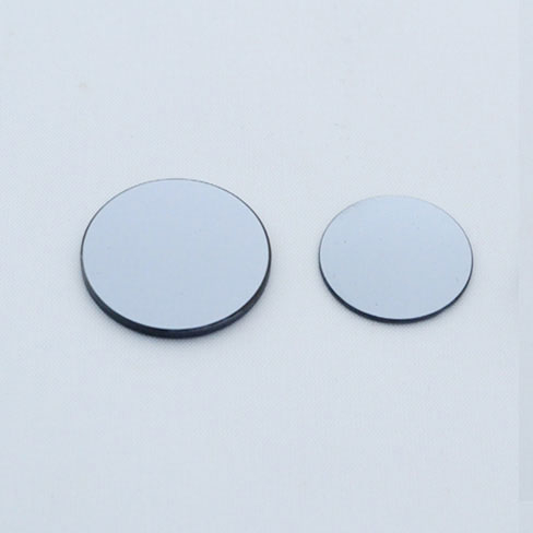
High Quality Best Price Silicon Material(Blank Substrate)--Flat Round plate
Add to Basket
More >>
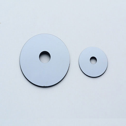
High Quality Best Price Silicon Material(Substrate)-Round plate w/aperture
Add to Basket
More >>
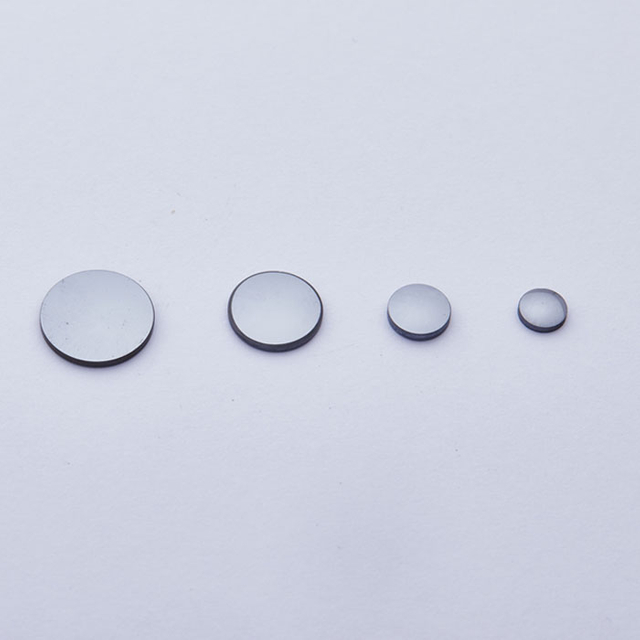
High Quality Best Price Silicon material(silicon lenses without AR Coating)
Add to Basket
More >>
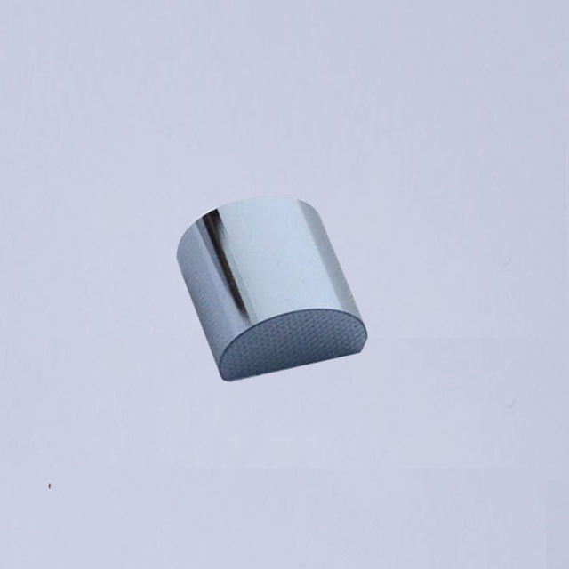
High Quality Factory Price Silicon Material(Blank Substrate)-Cylindrical
Add to Basket
More >>
QUICK LINKS
Home
Encoder
Optical Lens
Customization
About Us
Service & Support
News
Contact Us
Sitemap
Privacy Policy
ENCODER
Absolute Encoder
Incremental Encoder
Sincos Encoder
Rotary Encoder
Optical Encoder
Hollow Shaft Encoder
Solid Shaft Encoder
Ultra-thin Encoder
Bearingless Encoder
High Protection Encoder
Servo Motor Encoder
High Pulse Encoder
OPTICAL LENS
Silicon Lens
Silicon Substrate
Germanium Lens
Infrared Lens
Colored Glass Filters
Optical Filter
Optical Lens
Cylindrical Lens
Optical Mirrors
Germanium Grain
Germanium Material
Achromatic lens
Triangular Prism Lens
Sapphire Window
Quartz Window
CONTACT US
Tel:
+86-189-3007-7369/+86-021-5461-3487
Skype
:
lizwang07
E-mail:
fang@shhxgd.com
Address: Building7, Lane 115 (Chuangyi International Industrial Park), No.1276 Nanle Road, SongJiang, Shanghai,201600
Subscribe
+86-189-3007-7369
+86-021-5461-3487
+86-186-1688-3327
lizwang07
fang@shhxgd.com
Copyright 2025 © Shanghai Hengxiang Optical Electronics Co.,Ltd. All rights reserved Technology by
leadong.com

")